Microprocessor Vectored Interrupts
1.
SIM
2.
RIM
·
Microprocessor 8086 Architecture
1.
BIU
2.
EU
Microprocessor Vectored Interrupts
1. SIM
(Set Interrupt Mask)
2. RIM
(Ret/Read Interrupt Mask)
1. SIM
(Set Interrupt Mask)
This instruction reads the contents of the accumulator and enables or disables the interrupts consistent with the contents of the accumulator.
 |
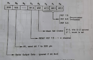
| SET INTERRUPT MASK |
The 1 in bit-6 enables the serial I/O and bit-7 are often send to SOD pin. The bit-4 is additional control for the RST 7.5. If bit-4=1, the RST 7.5 is disabled. The bit-3 may be a control bit and will be 1 to form lower three bits effective. The 0 in bit-2, bit-1 and bit-0 will
enable the corresponding interrupts and 1 will disable the interrupts.
Let
us write the sequence of instructions to enable all the interrupt of the 8085.
It is written as follows:
EI ; enable interrupts
MVI A, 08h ; load accumulator with
suitable bit pattern
SIM ; enable RST 7.5, RST 6.5 and RST 5.5
In above example, bit-4=1 within the accumulator makes the lower 3-bits effective. As 8085 has five interrupt pins, it is possible that while one
interrupt is under process, the 8085 receives the other interrupts on the lines
which are pending for execution. The RIM (Read Interrupt Mask) instruction
gives the detail of pending interrupts. It is discussed as follows.
2. RIM
(Ret Interrupt Mask)
This instruction loads the accumulator with the present status of the interrupt masks, the interrupt enable, pending interrupts and serial input file .
 |
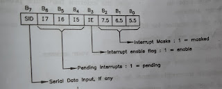
| RIM INTERRUPT MASK |
The
lower 3-bits show the current status of the RST 7.5, RST 6.5 and RST 5.5,
whether they are enabled or disabled. The next bit shows the status of
interrupt system of the processor as a group, whether it is enabled or
disabled. The EI instruction sets this flag to 1 and therefore the DI instruction resets it to 0. subsequent 3-bits show the pending status of the RST 7.5, RST 6.5 and RST 5.5, whether some or all of them are pending or not. The last bit may be a bit received from the SID (Serial Input Data) pin of the Processor, if it's available during the execution of the RIM instruction.
Let us assume that the RIM instruction loads the accumulator with the data byte 2Ch. what's meaning of it?
The accumulator is loaded with the binary number 0010 1100. If it's interpreted, the subsequent meaning evolves.
1.
RST 7.5 enabled, RST 6.5 and RST 5.5 disabled
2.
Interrupt system enabled
3.
RST 6.5 pending
Microprocessor 8086 Architecture
The
8086 Architecture is Intel’s first 16-bit processor introduced in 1978. Intel introduced some new concepts with 8086 which are mainly pipelining and memory segmentation.
The introduction of pipeline made 8086 Architecture of Microprocessor to perform operations at higher speed which reduced overall processing time considerably. The memory segmentation makes programs more manageable. The 8086 also introduced multiplication and division instructions as well as special instruction for string processing. The 8086 Microprocessor is fully 16-bit external data bus and addresses upto 1 MP memory with its 20-bit address bus (220= 1 MB).
The introduction of pipeline made 8086 Architecture of Microprocessor to perform operations at higher speed which reduced overall processing time considerably. The memory segmentation makes programs more manageable. The 8086 also introduced multiplication and division instructions as well as special instruction for string processing. The 8086 Microprocessor is fully 16-bit external data bus and addresses upto 1 MP memory with its 20-bit address bus (220= 1 MB).
1. Bus
Interface Unit (BIU)
2. Execution
Unit (EU)
 |
| DIAGRAM OF INTEL 8086 |
1. Bus Interface Unit (BIU)
The BIU is liable for interfacing 8086 Microprocessor Architecture with the external devices. BIU also computers addresses before it sends address on address bus. In short, it provides BIU contains following functional units.
1. Prefetch queue
2. Segment registers
3. Instruction pointer
They are
discussed as follows:
Prefetch
queue: it is 6-byte First-In-First-Out (FIFO) queue which may store upto 6 instruction bytes. The BIU fetches instruction bytes from memory before time and stores it in prefetch queue. Whenever execution unit completes execution of previous instruction, it receives next instruction from queue and starts executing it. As next instruction is quickly available in queue, EU needn't await fetching the instruction. this protects considerable time and speed up execution. The concept of fetching instructions before time and storing it in queue which is employed by EU whenever it's free, is understood as pipelining. The BIU
fetches instructions in sequence which causes problem when JMP or CALL
instruction comes. In case of JMP or CALL, the execution will not continue in
sequence, but the control will be transfer red
to target of JMP or CALL and execution should continue from new location. To
avoid this problem, whenever execution unit executes JMP or CALL instruction,
prefetch queue is made empty and it is filled up again from new location. The concept of instruction pipeling is discussed intimately in section.
Segment
registers: The BIU has four segment registers as follws:
Code Segment register
Data Segment register
Stack Segment register
Extra Segment register
The total memory accessed by 8086/88 is 1 MB (220
= 1 MB). It divides 1 MB memory into chunks of 64 KB and at a time it accesses just one of the 64 KB chunk. The 16-bit base address of 64 KB chunk (called segment) is stored in one among the segment register. All four segment register are of 16-bit.
Instruction
Pointer (IP): It is a 16-bit register which stores offset (logical) address
of next instruction to be executed.
2. Execution Unit(EU):
The execution
unit executes an instruction while BIU is fetching another instruction or data
from memory which makes two units works parallel to improve performance. Once execution unit completes execution of current instruction, it reads next instruction from prefetch queue. The EU also tells BIU whenever it needs some data to be read from memory or written into memory as a neighborhood of execution of current instruction. the most functions of EU are telling BIU from where to fetch information, decoding instruction and executing instructions. the main components of EU are
1. Control circuit
2. Instruction decoder
3. ALU
4. General purpose register
5. Stack pointer
6. Index register
7. Flag register
The negative feedback circuit controls all the operators performed by the processor. The Instruction decoder decodes the instruction and divide an instruction into small steps required to execute it. The 16-bit ALU performs all the arithmetic and logical operations. The registers provide memory space for operands.
General
purpose registers: The 8086 Microprocessor Architecture has four 16-bit general purpose registers namely AX, BX, CX and DX. Each of them are often also used as two 8-bit registers i.e. AX are often used as AH and AL, BX are often used as BH and BL, CX are often used as CH and CL and DX are often used as DH and DL. AH is higher byte of AX register while AL is lower byte of AX register. Same is for BX, CX and DX.
The AX register
is known as accumulator of 8086 Architecture and used as default register in some
instructions like multiplication and divison. The CX register is used as
counter in looping and repeat instructions and hence sometimes also known as
count register. The BX register is called base register as it is frequently
used as pointer to memory location. The DX register is referred as data
register. It is also used as I/O address pointer in IN and OUT instructions.
Stack
pointers: A 16-bit register SP (stack pointer) is employed to store offset address of top of stack where last value is stored. The 8086 Architecture of Microprocessor has another stack pointer referred to as BP (Base pointer). it's also used with stack segment and really useful in parameter passing and accessing during subroutine execution.
Index
registers: the 8086 has two more 16-bit registers referred to as index registers. they're SI (source Index) and DI (Destination Index). they will be used only as 16-bit registers. they will be used as general purpose registers or as index registers to stay track of index values in arrays. The SI and DI registers are used inherently in string instructions to point to source and destination strings respectively.
Flag register: it is a 16-bit register and contains.
Overflow
flag, Direction flag, Trap flag, Sign flag, Carry flag, Parity flag, Auxiliary
Carry flag, Zero flag, Interrupt flag.
The conditional
flags are set or reset according to execution of arithmetic and logical
instructions. They are used as condition in branch instructions and very useful
for flow control. The control flags are wont to control behavior of processor itself. they will be set or reset by special instructions. for instance , STI is employed to line interrupt flag to 1 and CLI is employed to clear it.
The TF (Trap flag) is beneficial for single stepping of problem during debugging and employed by debugging tools. The IF (Interrupt flag) is employed to enable or disable maskable interrupts. If If is 0, 8086 Microprocessor ignores maskable interrupts occur on INTR
pin. The CLI (Clear Interrupt) and STI (Set Interrupt) instruction are wont to clear or set IF flag respectively. it's almost like EI and DI instructions of 8085 microprocessor. The DF (Direction flag) is beneficial in string operations. If DF=0, then index registers are incremented, and if DF=1, they're decremented. The CLD and STD instruction are wont to clear and set direction flag respectively.

Post a Comment
Please do not enter any spam link in the comment box.